Nanonets: the fourth form of materials
Materials come in different shapes and forms, these lead to different application opportunities. Nanowires can be regarded as a new form of matter. As an example silicon has three well studied and known forms: single crystal, polycrystalline and amorphous silicon – with the three forms having different properties and thus different application opportunities. A silicon Nanonet, in turn can be regarded as the fourth form, with unique properties and applications on it’s own right.
The wires the group is investigating are highly conducting and there is a (tunable) barrier that limits the charge propagation from wire to wire. At any finite temperature there is a transition from a non-conducting to conducting state at the percolation transition with increasing network density. Above this critical density, at high temperatures transport proceeds through thermally assisted hopping between barriers, leading to a classical percolation problem, while at low temperatures tunneling between the different segments determines that conducting process, placing such systems in the quantum transport and quantum phase transition limit displaying a quantum (localization) phase transition with increasing network density. Thus the three states of such system are non-conducting (below the percolation threshold at NP), localized (above NP but below the localization transition NQ) and delocalized at densities above NQ
Nanonets also offer ample application opportunities, ranging from printed electronics and power storage. In addition, in combination with other materials, applications in diverse areas, from optoelectronics to sensors arise. The group is at the forefront of research in this area.
More information can be found in the following documents:
Nanowire and carbon nanotube networks
A combination of novel architectures, materials and fabrication routes, together with a host of electrical and optical measurements are pursued by the group in the area that, in general can be called transparent and flexible electronics.
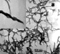
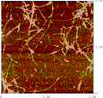
Architecture - The fundamental architecture is that of a random molecular nanowire network that serves as the conducting channel for a variety of optically transparent films and electronic devices. An appropriate analogy of the architecture is that of an interconnected network of freeways, providing a fast transport medium for electrons – potentially significantly faster than a uniform, but lower conductivity medium (analogous to surface roads or the terrain itself). Our focus is on a two dimensional network of conducting nanoscale wires, with carbon nanotubes as the main example. Initial studies by us have established some new properties of such networks, in particular near to the so-called percolation threshold, defined as the network density where conducting commences, with progressively increasing network density. At network densities, beyond the threshold the conduction displays well defined functional dependence on the density. In addition to the DC properties, observed at low voltages, the conductivity is expected to be frequency and voltage dependent. In the other side of the percolation threshold, unusual dielectric properties are expected, with a divergent dielectric constant at the percolation threshold.
Materials - The materials used include extremely highly conducting, and mechanically robust nano-scale wires, with carbon nanotubes as the prime example. The intitial focus will be on networks based on carbon nanotubes, nanoscale wires with extremely high electron and hole mobilities. Here, because of the high mobility, a rare network has substantial conductivity, and is, at the same time transparent. Initial work by us has demonstrated networks with superior mobilities, and high current carrying capacity. While carbon nanotubes possess excellent electronic characteristics, work at UCLA has demonstrated that other nanostructures, such as nanofibers and other molecular nanowires have the ability to act as highly conducting networks.
Room-temperature fabrication - Current nanowire deposition methods are largely based on high-temperature chemical vapor deposition processes that are incompatible with standard interconnect technology and with the substrates required for flexible electronics. Working with carbon nanotubes as the most promising materials for short-term applications, a variety of superior, room-temperature fabrication techniques have been explored and demonstrated at UCLA. These fabrication routes enable large-area conducting transparent layer fabrication using cheap and simple printing or spraying processes on a variety of surfaces, including transparent substrates and polymers.
Passive and active electronic devices. The architecture supports both a conducting networks, but also conducting channels of active electronic devices such as diodes and Field Effect Transistors (FETs), with an intimate connection between the fundamental network parameters and the parameters that determine the operation of the devices.
Merging electronics with chemistry and biology. The devices can be combined with chemical and biological species, that lead to interesting interaction between electronics and chemistry/biology. Typical examples include light sensitive molecules – leading to opto-electronics and solar cell applications – together with DNA and protein attachment – the fundamentals behind biosensing.
Application potential. While our focus is on fundamental
issues of a two dimensional conducting network, the novel, transparent and
electrically conducting architecture, as an application platform promises to
have a major impact on a variety of areas where the cheap fabrication more than
compensates for the compromise in performance. Network platform application examples include
optically transparent conducting thin films (NTCOND) and field effect
transistor (NETFET) devices that use carbon nanotubes as the
conductive channel.