3D atomic positions and crystal defects in quantum materials
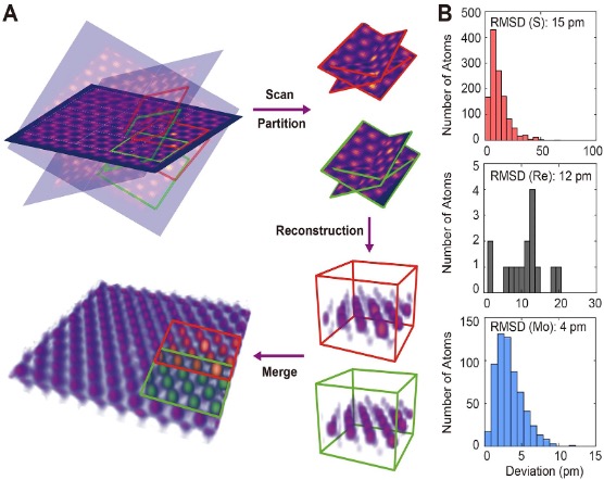
2D materials and heterostructures exhibit exceptional electronic, optical, and chemical properties, with potential applications ranging from electronics and photovoltaics to quantum information science. However, these properties are strongly dependent on the 3D atomic structure of the materials and, crucially, the presence of crystal defects. Using Re-doped MoS2 as a model, we have developed scanning AET (sAET) to determine the atomic positions and crystal defects such as dopants, vacancies, and ripples, with a 3D precision down to 4 picometers (Fig. 1).
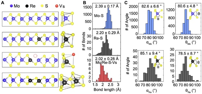
From the experimental 3D atomic coordinates, we characterized the 3D bond distortion induced by the single dopants. We observed that the Re-Re pair and the Re-S vacancy pair induce larger distortion than single Re dopants (Fig. 2A). The Mo-S and Re-S bond length was measured to be 2.39±0.17 Å and 2.20±0.29 Å, respectively (Fig. 2B). Statistically, the Re-S bond is 19 pm shorter than the Mo-S bond. With S vacancies, the opposite Re/Mo-S bond length was reduced to 2.02±0.28 Å (Fig. 2B). We found that a large fraction of the S vacancies are situated next to the Re dopants, which is due to the lower vacancy formation energy of neighboring Re dopants. We also measured the deviation of the bond angles from the 1H structure. The angles between the Re-S bonds in the same and opposite atomic layer are 85.1±9.4˚ and 78.5±8.7˚, respectively, whereas the corresponding angles of the Mo-S bonds are 82.6±6.6˚ and 80.6±4.8˚ (Fig. 2C).
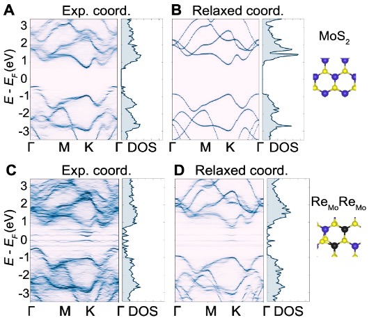
To correlate the 3D crystal defects with the electronic band structure of the Re-doped MoS2 monolayer, we used the experimental 3D atomic coordinates as direct input to density functional theory (DFT) calculations to derive the effective band structure (Fig. 3A and C). For comparison, the same experimental atomic coordinates were relaxed to obtain the equilibrium band structures by DFT (Fig. 3B and D). The band structures obtained directly from the experimental coordinates show metal-like behavior with a large number of shadow bands. In contrast, the band structures of the relaxed experimental coordinates exhibit direct band gaps with significantly reduced shadow bands. This behavior is consistent throughout the Brillouin zone as seen in the density of states (DOS) shown to the right of each band structure (Fig. 3). In addition to the shadow bands, we also observed defect states in the band structure of the supercell containing Re dopants (Fig. 3B). The striking differences between the band structures of the experimental and relaxed atomic coordinates suggest that the experimental structure is in a metastable state due to the complex strain distribution induced by 3D crystal defects and the interactions with the rest of the lattice, while the relaxed structure is in the global equilibrium state. The metastable structure is feasible as Re dopants in MoS2 produce defect wave functions that delocalize with slowly decaying tails. This delocalization of defect states with increasing concentration in various clusters of dopants results in a metastable structure, which clearly exhibits different electronic band structures (Fig. 3).
To experimentally study the effect of the band structure, we measured photoluminescence (PL) of Re-doped MoS2 and pristine MoS2 monolayers synthesized under the same conditions. Compared to the pristine MoS2 data, we observed that the PL spectrum of Re-doped MoS2 exhibits much lower peak intensity with the peak position only slightly shifted towards lower energies. This observation is consistent with our effective band structure calculations, indicating that the Re-doped MoS2 monolayer is a highly distorted indirect band gap semiconductor (Fig. 3A and C). This work demonstrates the necessity and importance of directly providing experimental 3D atomic coordinates to DFT to reveal electronic properties of a 2D materials in metastable states, whereas ab initio calculations relying on relaxed 3D atomic models can only predict material properties in the equilibrium state. With the increase of computational power in the future, the complete set of experimental 3D atomic coordinates determined by sAET can be used as direct input to DFT calculations to correlate 3D crystal defects with the electronic properties of 2D materials.
Selected Publications
1. X. Tian, D. S. Kim, S. Yang, C. J. Ciccarino, Y. Gong, Yo. Yang, Ya. Yang, B. Duschatko, Y. Yuan, P. M. Ajayan, J. C. Idrobo, P. Narang and J. Miao, "Correlating the three-dimensional atomic defects and electronic properties of two-dimensional transition metal dichalcogenides", Nature Mater. 19, 867-873 (2020).
2. X. Tian, X. Yan, G. Varnavides, Y. Yuan, D.S. Kim, CJ. Ciccarino, P. Anikeeva, M.-Y. Li, L.-J. Li, P. Narang, X. Pan, and J. Miao, Sci. Adv. 7, eabi6699 (2021).
3. Q. Ji, C. Su, N. Mao, X. Tian, J.-C. Idrobo, J. Miao, W.A. Tisdale, A. Zettl, J. Li, and J. Kong, "Revealing the Brønsted-Evans-Polanyi relation in halide-activated fast MoS2 growth toward millimeter-sized 2D crystals", Sci. Adv. 7, eabj3274 (2021).
4. M. Bian, A.N. Kamenskii, M. Han, W. Li, S. Wei, X. Tian, D.B. Eason, F. Sun, K. He, H. Hui, F. Yao, R. Sabirianov, J.P. Bird, C. Yang, J. Miao, J. Lin , S.A. Crooker , Y. Hou, and H. Zeng, "Covalent 2D Cr2Te3 ferromagnet", Mater. Res. Lett. 9, 205–212 (2021).
5. P. Ci, X. Tian, J. Kang, A. Salazar, K. Eriguchi, S. Warkander, K. Tang, J. Liu, Y. Chen, S. Tongay, W. Walukiewicz, J. Miao, O. Dubon, and J. Wu, "Chemical trends of deep levels in van der Waals semiconductors", Nat. Commun. 11, 5373 (2020).